Custom FR4 ENIG Double Side PCB Assembly for Control Series Products
Double Side PCB Assembly Introduction
Double-sided PCB Assembly are mainly used for electronic computers with high electronic communication equipment requirements, advanced instruments, and performance. It is usually punched in the middle of the circuit board to connect the double-sided PCB board.
PCB CAPABILITIES
| No. | Items | |
| 1 | HDI Capabilities | HDI ELIC(5+2+5) |
| 2 | Max layer count | 36L |
| 3 | Board Thickness | Core thickness 0.05mm-1.5mm ,Fineshed board thickness0.3-3.5mm |
| 4 | Min.Hole Size | Laser 0.05mm |
| Mechnical 0.15 |
| 5 | Min Line Width/Space | 0.030mm/0.030mm |
| 6 | Copper Thickness | 1/3oz-6oz |
| 7 | Size Max Panel size | 700x610mm |
| 8 | Registration Accuracy | +/-0.05mm |
| 9 | Routing Accuracy | +/-0.05mm |
| 10 | Min.BGA PAD | 0.125mm |
| 11 | Max Aspect Ratio | 10:01 |
| 12 | Bow and Twist | 0.50% |
| 13 | Impedance Control Tolerance | +/-5% |
| 14 | Daily output | 4,000m2 (Max capacity of equipment) |
| 15 | Surface Finishing | ENEPING /ENIG /HASL /FINGER GOLD/IMMERSION TIN/SELECTIVE THICK GOLD |
| 16 | Raw Material | FR-4/Normal Tg/High Tg/Low Dk/HF FR4/PTEE/PI |
PCBA CAPABILITIES
| PCBA Capability |
| Material type | PCB | Components |
| Item | Dimension (Length, width,height. mm) | Material | Surface finish | Chip&IC | BGA Pitch | QFP Pitch |
| Min | 50*40*0.38 | FR-4,CEM-1,CEM-3,Aluminium-based board,Rogers,ceramic plate,FPC | HASL, OSP, Immersion gold, Flash Gold Finger | 1005 | 0.3mm | 0.3mm |
| Max | 600*400*4.2 | | |
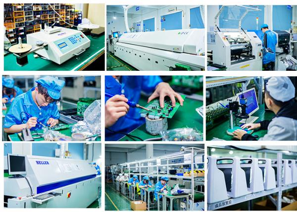
PCB Assembly Process
1.Solder Paste stenciling---2.Surface Mount Technology (Pick and Place)---3.Reflow Soldering---4.Inspection and Quality Control---5.Through-Hole Component Insertion (DIP Process)---6.Final Inspection and Functional Test

Our advantage
1.Service value
Independent quotation system to quickly serve the market
2.PCB manufacturing
High-tech PCB and PCB assembly production line
3.Material purchasing
A team of experienced electronic component procurement engineers
4.SMT post soldering
Dust-free workshop, high-end SMT patch processing

Double Side PCB Assembly Delivery Time
| Product Type | Qty | Normal lead time | Quick-turn lead time |
| SMT+DIP | 1-50 | 1WD-2WD | 8H |
| SMT+DIP | 51-200 | 2WD-3WD | 1.5WD |
| SMT+DIP | 201-2000 | 3WD-4WD | 2WD |
| SMT+DIP | ≥2001 | 4WD-5WD | 3WD |
| PCBA(2-4Layer) | 1-50 | 2.5WD-3.5WD | 1WD |
| PCBA(2-4Layer) | 51-2000 | 5WD-6WD | 2.5WD |
| PCBA(2-4Layer) | ≥2001 | ≥7WD | 5WD |
| PCBA(6-10Layer) | 1-50 | 3WD-4WD | 2.5WD |
| PCBA(6-10Layer) | 51-2000 | 7WD-8WD | 6WD |
| PCBA(10-HDILayer) | 1-50 | 7WD-9WD | 5WD |
| PCBA(10-HDILayer) | 51-2000 | 9WD-11WD | 7WD |
Why choose us?
1. We are the manufacturer/ factory; Welcome to visit us one day.
2. We have good quality control systems, including AOI, ISO 9001 etc. ;
3. All the material we use have the RoHS identify;
4. All the components we use are the New & Original;
5. One-stop service can be provided from PCB design, 1-36 layers PCB manufacturing, components sourcing, PCB Assembly, to Fully Product Assembly.

Double Side PCB Assembly Application Field
Printed circuit boards And PCB Assembly are mainly used for many communication industry, medical equipments, consumer electronics and automobile industry ,automotive electronics , audio and video, optoelectronics, robotics, hydroelectric power, aerospace, education, power supply, printer etc industries.

Our Workshop

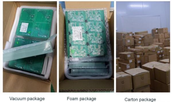
Common packaging
1.PCB: Vacuum packaging with carton box
2.PCBA: ESD packaging with carton box
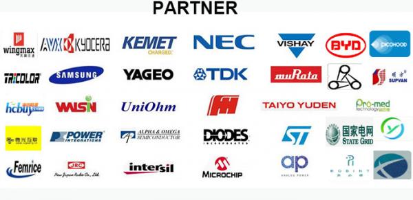
Partner
Product Tags:

|
|
FR4 ENIG Double Side PCB Assembly , 3OZ Customized PCB Assembly Images
|