FR-4 FPC Circuit Board Multilayer SMT craft Flex PCB Assembly
Flexible PCB Board Introduction
Flex boards can be used as connectors, and as full circuits assembled with components. And yes it can hold the soldering heat moreover it can stand way more than rigid ones with high temperature based on the used film material type.
Haina lean Electronics Co., Ltd produce HDI board, Fast PCB board, RF PCB board, PCBA, high frequencyPCB board ,high speed board and rigid-flex board, etc., to meet customers' various demands.
All our products follow IPC class and are approved by UL, ROHS and ISO9001.
Basic Information/Detail data
| FACTORY CAPABILITIES |
| No. | Items | 2019 | 2020 |
| 1 | HDI Capabilities | HDI ELIC (4+2+4) | HDI ELIC(5+2+5) |
| 2 | Max layer count | 32L | 36L |
| 3 | Board Thickness | Core thickness 0.05mm-1.5mm ,Fineshed board thickness 0.3-3.5mm | Core thickness 0.05mm-1.5mm ,Fineshed board thickness 0.3-3.5mm |
| 4 | Min.Hole Size | Laser 0.075mm | Laser 0.05mm |
| Mechnical 0.15mm | Mechnical 0.15mm |
| 5 | Min Line Width/Space | 0.035mm/0.035mm | 0.030mm/0.030mm |
| 6 | Copper Thickness | 1/3oz-4oz | 1/3oz-6oz |
| 7 | Size Max Panel size | 700x610mm | 700x610mm |
| 8 | Registration Accuracy | +/-0.05mm | +/-0.05mm |
| 9 | Routing Accuracy | +/-0.075mm | +/-0.05mm |
| 10 | Min.BGA PAD | 0.15mm | 0.125mm |
| 11 | Max Aspect Ratio | 10:1 | 10:1 |
| 12 | Bow and Twist | 0.50% | 0.50% |
| 13 | Impedance Control Tolerance | +/-8% | +/-5% |
| 14 | Daily Output | 3,000m2 (Max capacity of equipment) | 4,000m2 (Max capacity of equipment) |
| 15 | Surface Finishing | ENEPING /ENIG /HASL /FINGER GOLD/IMMERSION TIN/SELECTIVE THICK GOLD |
| 16 | Raw Material | FR-4/Normal Tg/High Tg/Low Dk/HF FR4/PTEE/PI |
Market Success:
Products are mainly exported to Europe and USA;
Our customers spread over more than 80 countries;
Products are widely used in various industries.

Flex PCB Assembly fabricating


Our service
Electronic Manufacturing Service
PCB Electronic Design
PCB Layout Service
PCB Supplier & Quality Inspection Service
PCBA Components Sourcing
PCB Assembly process service

Delivery Time
| Prototype PCB | Batch | Prototype | Expedited |
| Double sides | 9 Days | 5 Days | 45h |
| Four-layer | 10 Days | 5 Days | 3 Days |
| Six-layer | 12 Days | 6 Days | 3 Days |
| Eight-layer | 12 Days | 7 Days | 4 Days |
| Ten-layer | 14 Days | 10 Days | 4Days |
| Twelve-layer | 14 Days | 10 Days | 5 Days |
| Fourteen-layer | 16 Days | 12Days | 6 Days |
| Sixteen-layer | 16 Days | 12 Days | 6 Days |
| Eighteen-layer | 18 Days | 14 Days | 6 Days |
| Twenty-layer | 18 Days | 14 Days | 10 Days |
| Twenty two-layer | 20 Days | 14 Days | 10 Days |
| Twenty four-layer | 20 Days | 14 Days | 10 Days |
| Twenty six-layer | 20 Days | 14 Days | 10 Days |
| Twenty eight-layer | 20 Days | 14 Days | 10 Days |
FR4 Multilayer Bare Printed Circuit Board PCB Application Field
Printed circuit boards and PCB Assembly are widey used in many communication industry, power, security, optoelectronics, industrial control, medical equipments, consumer electronics and automobile industry etc field.

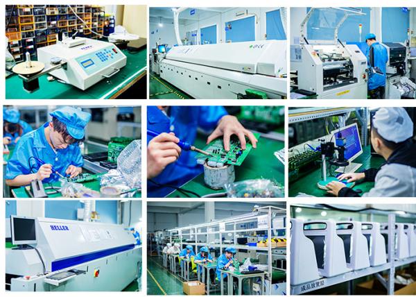
Workshop


Testing service
1. Manual visual inspection of PCB board
2. PCB board online test
3. PCB board function test
4. AOI (Automatic optical inspection)
5. Automatic X-ray inspection
6. Laser detection system
7. Size detection
Above is the PCB testing service.
Haina lean Electronics provides custom test service according to client's requirements and products.
Usually Haina lean Electronics Co.,Ltd PCBA Tech offers a full range of testing service. Including:
1. AOI(Automatic Optical Inspection)
2. Function Testing
3. In Circuit Testing
4. Testing Jig
5. Testing Service
6. X-Ray for BGA Testing
7. Printing Solder Paste Test
Each board is carefully examined by our dedicated inspection team using AOI and high magnification viewers.
Using our X-Ray machine, we test PCBs to component level and all wiring is fully inspected and tested.
Flash testing and earth bonding tests can also be undertaken where required.
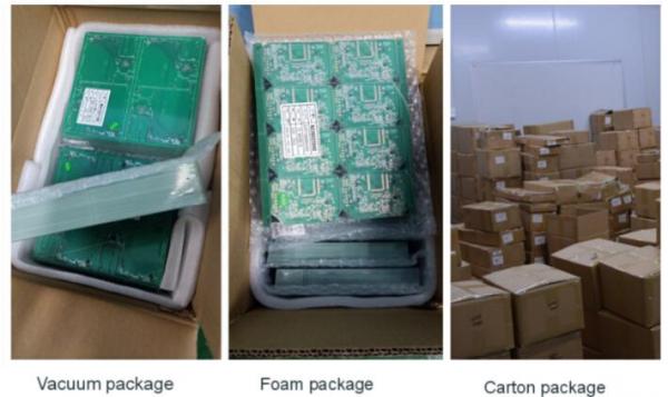
Common packaging
PCB: Vacuum packaging with carton box
PCBA: ESD packaging with carton box
Why choose us?
Welcome to visit our factory, Haina lean Electronics Co., Ltd.
1. Experienced: Focus on PCB And PCBA munufacturing over 10 years.
2. Professional: Expertise engineer with barrier-free English
3. Rapid delivery: On-time delivery rate reaches 98%
4.Cost effective: No excessive profits. Lower cost with same quality And service
FAQ
Q1.
What's your MOQ ?
No Moq ,We accept small orders as well as mass production.
Q2.
For small quantity orders, can you produce prototype PCB?
Haina lean Electronics Co., has the capability to produce circuit boards in any amount.
Q3.
Can You provide fast rotating PCB ?
Yes , we can provide fast service 24 hours .
Q4.
What are the services you can provide ?
One-stop contract manufacturing
PCB board, PCB Design & Layout, PCB Assembly, PCBA programming & functional testing, Electronic components purchasing service, Enclosure molding & final assembly with labels,instructions,enclosure, boxes.
Q5.
Whether all PCBA s will be tested before delivery ?
Yes , we will test each piece of PCBA product under your testing methods ,to ensure quality and functionality .
Q6.
Do you provide OEM service ?
Yes ,we offer PCB and PCBA OEM Service , we manufacture the PCB and PCBA products to your design and requirements .
Q7.
Shipping Cost ?
The shipping cost is determined by the destination ,weight ,packing size of the goods .We can provide shipping, air, land, express and other transportation services .
Q8.
Do you accept process materials supplied by clients?
Yes, we can provide component source, and we also accept component from client. OEM and ODM orders are accepted.
Company Information
Haina lean Electronics Co., Ltd is a one-stop EMS supplier integrating PCB design, PCB manufacturing, Component sourcing and PCB assembly.
The company is specialized in electronic products supporting processing services, mainly to undertake circuit board design, layout production, components procurement, PCB plate making, circuit board welding assembly debugging and other OEM/ODM services. A professional and reliable one-stop PCB solutions provider for customers specialized in manufacturing quick turn prototypes and small volumes. Haina lean Electronics is responsible for overseas business development.With high quality and on-time delivery products we won the market's wide acclaim. We are continuing to focus on customer satisfaction, along with "high quality "and "fast delivery", become a PCB service provider worthy of customer trust. The company pursues "inclusiveness, excellence, people-oriented".
Our customers are from over more than 80 countries. At present, the main cooperation industries are automotive electronics, communications, audio and video, optoelectronics, robotics, hydroelectric power, medical care, aerospace, education, radio frequency, power supply, printer etc industries.

Product Tags:

|
|
FR-4 FPC Circuit Board Multilayer SMT Flex PCB Assembly Images
|